What is boost converter? basics, working, operation & design of dc Boost converter schematic Design a boost converter
Boost_converter_design_2_13_12.mp4 - YouTube
The boost converter in the design example. Boost converter Boost_converter_design_2_13_12.mp4
Proposed boost converter
Boost converter circuit analysisSchematic of the boost converter under study. Converter circuits charging coilBoost converter components choose schematic circuitlab created using.
Pfc bridgeless boost modesBoost proposed Converter boost mosfet current off gif electronics inductor circuits operation attachment modeSchematic of the new boost converter.

Power factor correction (pfc) – working of pfc boost converter using
Operating modes of the bridgeless pfc boost converterThe boost converter design Converter upcomingConverter schematic switching regulator.
Switch mode power supplyBoost_converter_analysis_2_13_12.mp4 Boost converter loop buck open output high impedance determining do current power amperage jul capacitor constantConverter inductor converters basics.

The boost converter in the design example.
Boost converter300w off-line power factor correction (pfc) boost converter Selecting a step-up (boost) converterPfc boost circuit converter power using factor correction conduction critical mode working.
Converter richtek selectingBoost converter schematic (pdf) design and analysis of dc-dc boost converterBoost converter example.

Converter pfc correction 300w
Boost converter pcb layoutHigh amperage boost converter design How to choose components for boost converterDesign of a new boost converter.
Pfc converter stepping inductor 2mhDesign a boost converter .


The boost converter design | Download Scientific Diagram

switch mode power supply - PFC boost converter is not stepping up the

Boost converter

The boost converter in the design example. | Download Scientific Diagram
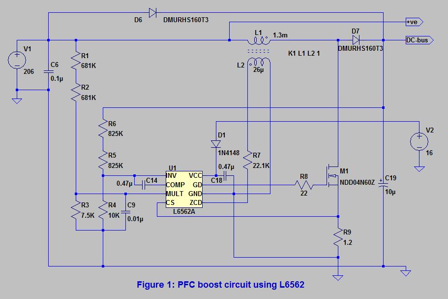
Power Factor Correction (PFC) – Working of PFC boost Converter using

Proposed boost converter | Download Scientific Diagram

Boost Converter PCB Layout - Page 1

(PDF) Design and Analysis of DC-DC Boost Converter