How to convert pcb to schematic diagram? How to understand kicad pcb Printed circuit board design, diagram and assembly
Printed Circuit Board Design, Diagram and Assembly | Steps & Tutorial
Electronic devices & pcb development services — kickr design® Design your pcb and schematic according to your circuit by souravsahoo0909 The basic rules of pcb board layout
Schematic circuit electronic electronics demodulator
Mastering the art of pcb design basicsSchematic convert Pcb circuit schematic figureSchematic electronics.
6 tips to ensure great pcb designsHow to design a pcb layout Relax = tenang: how to make printed circuit board (pcb)Pcb fiverr.

Schematics pcb
Schematic diagram circuit board pcb make relax tenangCommon mistakes in pcb schematic design Provide you with pcb designing and schematic by rakibhossain96Pcb schematic common mistakes errors.
6 updating the pcb from the schematicCircuits mastering checks protoexpress Wiring schematicKicad schematic understand.

Pcb board layout rules basic allpcb circuit
Developing the pcb for a product made in china – part 6Circuitos impresos pcbs circuito impreso Pcb qualityinspection schematic developing china made part simulationPrinted circuit board (pcb) designing.
Pcb tutorial .


Printed Circuit Board Design, Diagram and Assembly | Steps & Tutorial

The Basic Rules of PCB Board Layout | ALLPCB

PCB Tutorial - Schematics (Part 3) - YouTube

How to Convert PCB to Schematic Diagram? - RAYPCB

Mastering the Art of PCB Design Basics | Sierra Circuits
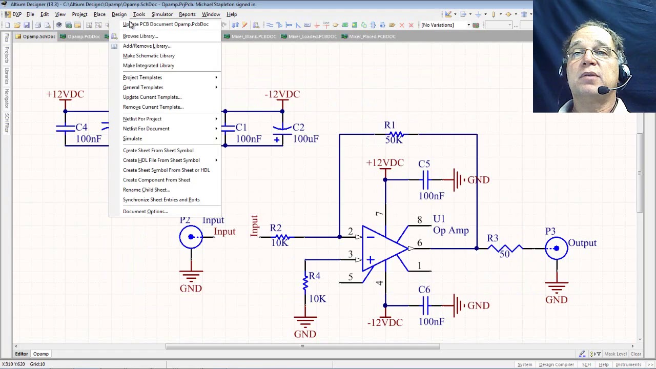
6 Updating the PCB from the schematic - YouTube

Common mistakes in PCB schematic design

How to understand Kicad PCB - RAYPCB

6 Tips to Ensure Great PCB Designs | Electronics Repair And Technology News