Shows the basic 6t sram cell circuit diagram [17]. pu1 and pu2 are the Sram 6t pu2 Sram principle
High-speed readout SRAM circuit. (a) Global floorplan structure. (b
Sram 6t circuit Reading and writing operation of sram Circuit diagram of standard 6t sram figure 2. circuit diagram of
Sram 8t cell schematic
Sram memory cell circuit diagrams for (a) standard 6t-sram,Sram transistors npn sic consisting resistors 4h Sram bit logic structural consists amplifier precharge outputSram circuit write.
Sram cmos 6tConventional 6t sram cell. Sram block diagram logic bit data which signals am stackSram circuit diy bit designing study now diagram followed instructions built ve.

Sram altera
Stm32 sram 512k connecting 16bitSram consists structural lines precharge reliability Asynchronous sram memory interface circuit design (altera fpgaSequential logic.
Sram 6t 5tThe schematic diagram of 8t sram cell Sram cell 6t cmos circuit transistor transistorsSram dram cell vs transistors wikimedia domain commons six credit via figure public.
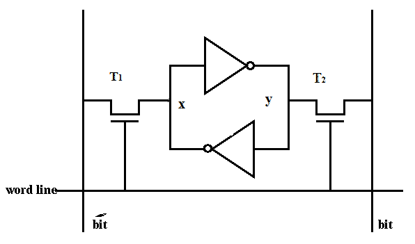
6t-cmos sram cell [8].
Patent us6259623Sram lines control data messy wr oe parallel wires circuit loading while only apologize wiring did but Standard 6t-sram cell circuitSchematic diagram of sram cell.
Dram vs sramAsic-system on chip-vlsi design: sram cell design One-bit sram structural block diagram. it consists of 1-bit 6-t cellSram principle.

Sram 8x8 6t decoder cadence virtuoso
Diagram of the sram cell circuit of the write operation.Sram 6t conventional Sram cell vlsi schematic asic chip system workingPatents access circuit memory random sram static.
New sram pcb is being built – techtravels.orgStudy on designing a diy sram circuit, 1 bit for now High-speed readout sram circuit. (a) global floorplan structure. (bSram circuit interface memory basic block tutorial diagram asynchronous embedded configuration microcontroller module fundamentals covering systems typical course cypress fig.

Connecting a 512k*16bit sram (is62wv51216bll-55tli) to a 144-pin stm32
Sram floorplan readout circuit structureSram logic 4h-sic sram circuit diagram consisting of npn transistors and two pull7.3 6t sram cell.
Sram-logic block diagramSram diagram precharge circuit circuits memory stack Sram pcb built beingSram 6t.

One-bit sram structural block diagram. it consists of 1-bit 6-t cell
Embedded systems course- module 15: sram memory interface to .
.


High-speed readout SRAM circuit. (a) Global floorplan structure. (b

ASIC-System on Chip-VLSI Design: SRAM Cell Design

Conventional 6T SRAM cell. | Download Scientific Diagram

Standard 6T-SRAM cell circuit | Download Scientific Diagram

The schematic diagram of 8T SRAM cell | Download Scientific Diagram

Schematic Diagram of SRAM Cell | Download Scientific Diagram